Heng An Standard Lif的問題,透過圖書和論文來找解法和答案更準確安心。 我們找到下列股價、配息、目標價等股票新聞資訊
Heng An Standard Lif的問題,我們搜遍了碩博士論文和台灣出版的書籍,推薦VITTACHI NURY寫的 青年科學家系列(一套12冊) 可以從中找到所需的評價。
另外網站Emerging Challenges and Solutions for Plastic Pollution也說明:... life cycle of fossil fuels ( oil , gas , and coal ) in relation to the life ... standard , used in common applications ( ~ 90 % Frontiers in Marine Science ...
長庚大學 電子工程學系 賴朝松所指導 Chintam Hanmandlu的 透明電極與介面工程於無遲滯之反式鈣鈦礦太陽能電池的特性研究 (2018),提出Heng An Standard Lif關鍵因素是什麼,來自於鈣鈦礦太陽能電池、透明電極、雙面、頂層照明、表面缺陷、介面、無遲滯。
而第二篇論文中原大學 物理研究所 邱寬城所指導 林恆信的 探討以NPB/AlQ3為基礎架構之不同的有機發光二極體之發光特性及介電性質 (2018),提出因為有 有機發光二極體、發光特性、介電特性、德拜鬆弛的重點而找出了 Heng An Standard Lif的解答。
最後網站Compliance job in Hong Kong at Heng An Standard Life (Asia ...則補充:Click here to view 1 Compliance job in Hong Kong at Heng An Standard Life (Asia) Limited, brought to you by eFinancialCareers.
除了Heng An Standard Lif,大家也想知道這些:
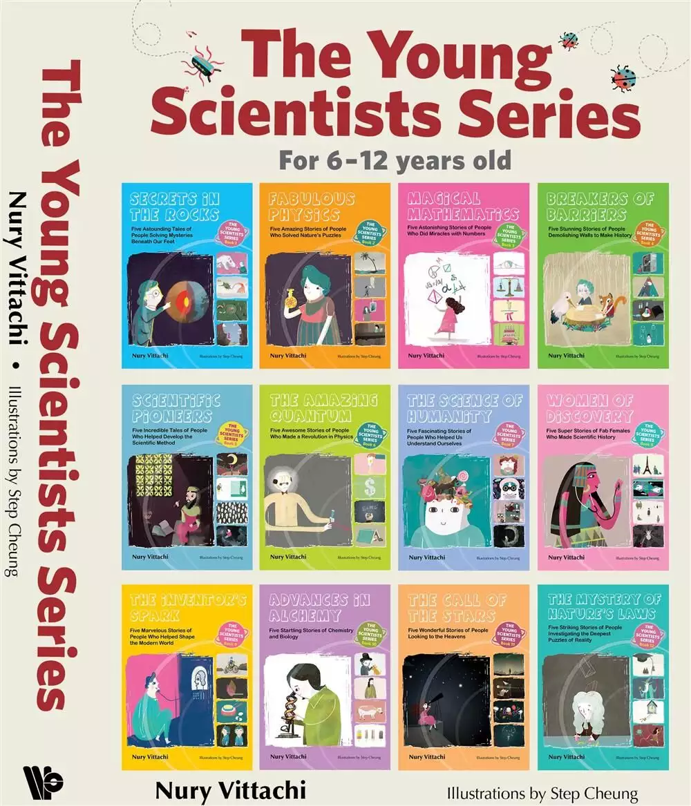
青年科學家系列(一套12冊)
為了解決Heng An Standard Lif 的問題,作者VITTACHI NURY 這樣論述:
Scientists are often presented as old men in white coats, but this series shows that great discoveries have been made by people of all ages and cultures ― some are young people, and many are female. 作者簡介 Nury Vittachi Nury Vittachi has authored of more than 40 books, several of whi
ch have been published in many languages around the world. He particularly enjoys bringing science and history to life for readers young and old. He is chairman of the Asia Pacific Translators & Writers, Inc., Asia''s biggest association of writers. A lecturer at the Hong Kong Polytechnic Uni
versity School of Design, he teaches students how to write stories and how to create content for novels and movies. 繪者簡介 Step Cheung Step Cheung studied Illustration at School of Visual Arts in NYC and Character Animation at Gobelins School in Paris. Her illustrations are published
in The Standard newspaper weekly and she has illustrated for McDonald''s TV commercials, Cyberport, HK magazines and different types of media. She loves to use variety of media to express her imagination of the world. Her dream is to draw every day. Volume 1: Secrets in the Rocks ― Five Asto
unding Tales of People Solving Mysteries Beneath Our Feet: The Girl Who Found a Flying Dragon (Mary Anning) The Boy Who Went Searching for Giants (Georges Cuvier) Love, Rocks and the First Dinosaur (Mary Morland) The Bug Boy Solves a Huge Mystery (Louis Agassiz) The Woman Who Saw Deep into
the Earth (Inge Lehman) Volume 2: Fabulous Physics ― Five Amazing Stories of People Who Solved Nature''s Puzzles: The Man Who Saw a Living Skeleton (Wilhelm Rontgen) The Servant Girl Who Beat Einstein (Marie Curie) The Boy Who Climbed to the Top (Abdus Salam) The Quiet Queen of Physic
s (Wu Chien-Shiung) The Boy Who Secretly Read the Books He Was Binding (Michael Faraday) Volume 3: Magical Mathematics ― Five Astonishing Stories of People Who Did Miracles with Numbers: The Girl, the Pearl and the Not-So-Sad Story (Lilavati) The Boy with No Birthday (Carl Gauss) The M
ath Girl Who Stunned the World (Philippa Garrett) The Penniless Youth Who Amazed the Professors (Srinivasa Ramanujan) The Good Witch Who Made an Amazing Decision (Maria Agnesi) Volume 4: Breakers of Barriers ― Five Stunning Stories of People Demolishing Walls to Make History: The Unloved
Teenager Who Found Her Place (Ada Byron Lovelace) The Scientist and the Secret in the Ancient Book (Tu Youyou) The Impossibly Young Doctors (Balamurali Ambati and Sho Timothy Yano) The Motherless Child Who Solved His Father''s Problem (Blaise Pascal) The Girl Torn Between Two Careers (Rache
l Carson) Volume 5: Scientific Pioneers ― Five Incredible Tales of People Who Helped Develop the Scientific Method: The Woman Who Hid the Moon (Aglaonike) The Man Who Stayed in His House for Ten Years (Al-Haytham) The Boy Who Was Curious All His Life (Shen Kuo) The Grumpy Nun Who Was F
orbidden to Sing (Hildegard of Bingen) The Boy Who Sorted Out the Living World (Carl Linneaus) Volume 6: The Amazing Quantum ― Five Awesome Stories of People Who Made a Revolution in Physics: The Boy Who Didn''t Listen to His Teacher (Max Planck) How a Compass Inspired a Genius (Albert E
instein) The Boy Secretly Reading a Book Behind His School Desk (Wolfgang Pauli) The Student Whose Schools Kept Closing (T D Lee) The Boy Who Had a Dispute with His Father (John von Neumann) Volume 7: The Science of Humanity ― Five Fascinating Stories of People Who Helped Us Understand O
urselves: The Boy Who Found Different Ways of Thinking (Jean Piaget) The Woman Who Taught Us Love and Remembrance (Artemisia) The Mother with Six Boys and Six Girls (Lillian Gilbreth) The Girl Born in the Shadow of the Moon God (Enheduanna) The Explorer Girl Who Travelled Far Without Leavi
ng Home (Alice Hamilton) Volume 8: Women of Discovery ― Five Super Stories of Fab Females Who Made Scientific History: The Girl Who Found Her Sisters on the Other Side of the World (Harriet Noyes) The First Woman Doctor in History (Merit Ptah) The Girl Who Had to Hide Behind a Man''s Nam
e (Sophie Germain) The Murderous Princess Who Found Salvation (Anna of Byzantium) The Bug Hunter Who Dreamed of the Jungle (Maria Merian) Volume 9: The Inventor''s Spark ― Five Marvelous Stories of People Who Helped Shape the Modern World: The Boy Who Combined a Bike and a Train to Inven
t the Car (Karl Benz) The Failed Doctor Who Sparked an Idea (John Walker) The Woman to Thank If You Like Chocolate (Mary the Alchemist) The Man in the Burning House (Garrett Morgan) The Boy Who Lost His Chance but Got It Back (Gregorio Zara) Volume 10: Advances in Alchemy ― Five Startl
ing Stories of Chemistry and Biology: The Strange Adventures of Doctor Poison (F F Runge) The Young Woman Who Was Forgotten (Rosalind Franklin) The Girl in the Chamber of Corpses (Alessandra Giliani) The Farm Girl Who Made Your Milk Safe (Alice Evans) A Tasty Treat Found by Accident (Frank
Epperson) Volume 11: The Call of the Stars ― Five Wonderful Stories of People Looking to the Heavens: The Boy Who Decoded the Dance of the Stars (Jeremiah Horrocks) The Poet–Scientist Who Detected an Earthquake (Zhang Heng) The Farm Boy Who Saw the Galaxies Flying Away (Vesto Slipher)
The Girl Who Named the Stars in the Sky (Annie Jump Cannon) The Boy Who Understood Einstein (Michio Kaku) Volume 12: The Mystery of Nature''s Laws ― Five Striking Stories of People Investigating the Deepest Puzzles of Reality: The Girl at the Back of the Boys-Only Classroom (Amalie Emmy N
oether) The True Story of the Philosopher''s Stone (Jabir Ibn Hayyan) The Bullied Boy Who Fought Back (Isaac Newton) The Teenager Who Saw the Light (Galileo Galilei) What We Learn from the Strange Tale of the Human Computer (Shakuntala Devi)
透明電極與介面工程於無遲滯之反式鈣鈦礦太陽能電池的特性研究
為了解決Heng An Standard Lif 的問題,作者Chintam Hanmandlu 這樣論述:
Table of ContentsThesis/Dissertation recommendation letter from advisor-------------------------------------------------Thesis/Dissertation oral defense committee certification-------------------------------------------------Acknowledgement ----------------------------------------------------------
--------------------------------iiiAbstract ------------------------------------------------------------------------------------------------------viTable of content -------------------------------------------------------------------------------------------viiiList of figures ------------------------
----------------------------------------------------------------------xiiiList of tables ----------------------------------------------------------------------------------------------xxiv1. Chapter 1: Introduction---------------------------------------------------------------------------------11.1
Solar cells -------------------------------------------------------------------------------------------------------11.2 Inorganic-organic hybrid perovskite solar cells -----------------------------------------------------------21.2.1 Device structure -----------------------------------------
---------------------------------------------41.2.2 Working Principle ------------------------------------------------------------------------------------41.3 Perovskite solar cell device characteristics ----------------------------------------------------------------61.3.1 Short circuit c
urrent density -------------------------------------------------------------------------61.3.2 Open Circuit voltage ---------------------------------------------------------------------------------71.3.3 Fill Factor ------------------------------------------------------------------------------
----------------71.3.4 Power conversion efficiency ------------------------------------------------------------------------81.4 Perovskite films fabrication techniques and device architectures----------------------------------------81.4.1 Perovskite layer preparation -----------------------
-------------------------------------------------81.4.1.1 Solution processing technique ------------------------------------------------------------------81.4.1.2 Vapor deposition technique ---------------------------------------------------------------------91.4.2 Device architectures ----
----------------------------------------------------------------------------101.4.2.1 Conventional n-i-p perovskite solar cells ----------------------------------------------------111.4.2.2 Inverted perovskite solar cells ----------------------------------------------------------------131.5
Interface engineering in perovskite solar cells------------------------------------------------------------141.5.1 Interface engineering--------------------------------------------------------------------------------141.5.1.1 Bang alignment ----------------------------------------------------
-----------------------------141.5.1.2 Carrier transportation --------------------------------------------------------------------------151.5.1.3 Carrier recombination --------------------------------------------------------------------------171.5.2 Interfacial materials -------------------
--------------------------------------------------------------181.5.2.1 Interfacial layers/Transport materials --------------------------------------------------------181.5.2.2 Interfacial materials/metal electrodes --------------------------------------------------------191.5.2.3 Interfaci
al materials/Transparent conducting oxides --------------------------------------191.5.2.4 Perovskite/HTL interface ----------------------------------------------------------------------201.6 Hysteresis in perovskite solar cells -----------------------------------------------------------------
-------211.6.1 Influence of charge traps --------------------------------------------------------------------------221.6.2 Band bending due to ferroelectric polarization -------------------------------------------------231.6.3 Ion migration --------------------------------------------------
--------------------------------------241.7 Transparent electrode design for semitransparent and ITO-Free perovskite solar cells ------------241.7.1 Transparent electrodes ------------------------------------------------------------------------------241.7.2 Semitransparent perovskite solar
cells -----------------------------------------------------------261.7.2.1 Transparent electrode --------------------------------------------------------------------------271.7.2.2 Perovskite film formation ---------------------------------------------------------------------281.7.2.3 Catho
de and anode modification -------------------------------------------------------------281.7.3 ITO-free perovskite solar cells --------------------------------------------------------------------291.8 Objectives and scopes -----------------------------------------------------------------------
----------------292. Chapter 2: Experimental section -------------------------------------------------------------------------------312.1 Bifacial perovskite solar cells featuring semitransparent electrodes ----------------------------------312.1.1 Methylammonium iodide preparation -----------------
--------------------------------------------312.1.2 Bifacial perovskite solar cells fabrication ---------------------------------------------------------312.1.3 Optical simulations -----------------------------------------------------------------------------------322.1.4 Characterizations ----------
---------------------------------------------------------------------------322.2 Top illuminated hysteresis-free perovskite solar cells incorporating microcavity structures onmteal electrodes: A combined experimental and theoretical approach ---------------------------------332.2.1 Solar cells devic
e fabrication ------------------------------------------------------------------------332.2.2 Optical simulations ------------------------------------------------------------------------------------342.2.3 Characterizations ----------------------------------------------------------------------------
----------342.3 Suppression of surface defects to achieve hysteresis-free inverted perovskite solar cells quantumdots passivation -----------------------------------------------------------------------------------------------342.3.1 Materials required ------------------------------------------------
-------------------------------------342.3.2 CdS/ZnS quantum dots preparation -----------------------------------------------------------------352.3.3 CdSe/ZnS quantum dots preparation ---------------------------------------------------------------352.3.4 Solution preparations and device fabrication
------------------------------------------------------362.3.5 Characterizations --------------------------------------------------------------------------------------372.3.6 Density functional theory calculations -------------------------------------------------------------403. Chapter 3: Bifacial
perovskite solar cells featuring semitransparent electrodes ---------------------423.1 Overview ------------------------------------------------------------------------------------------------------423.2 Results and discussions ------------------------------------------------------------------------
-------------443.3 Final remarks -------------------------------------------------------------------------------------------------604. Chapter 4: Top illuminated hysteresis-free perovskite solar cells incorporating microcavity onstructures on metal electrodes: A combined experimental and theoretical
approach -624.1 Overview ------------------------------------------------------------------------------------------------------624.2 Results and discussions -------------------------------------------------------------------------------------654.2.1 Device architecture, transparent electrode and pe
rovskite morphology on cavity electrode------------------------------------------------------------------------------------------------------------------654.2.2 Experimental and theoretical approach -----------------------------------------------------------684.2.3 Photovoltaic performance of perovs
kite solar cells with doped MoO3 on cavity electrode------------------------------------------------------------------------------------------------------------------734.2.4 Hysteresis ------------------------------------------------------------------------------------------------754.2.5 Thin film c
haracterizations ----------------------------------------------------------------------------774.2.6 Photovoltaics performance of perovskite solar cells with various metal cavity electrodes ---834.2.7 Performance of flexible perovskite solar cells ----------------------------------------------------
--864.3 Final remarks ---------------------------------------------------------------------------------------------------895. Chapter 5: Suppression of surface defects to achieve hysteresis-free inverted perovskite solarcells via quantum dots passivation ---------------------------------------------
-----------------905.1 Overview -------------------------------------------------------------------------------------------------------905.2 Results and Discussions --------------------------------------------------------------------------------------925.2.1 Device architecture ---------------------
---------------------------------------------------------------925.2.2 Effects of surface morphology and electronic properties of perovskites with quantum dotsPassivation ------------------------------------------------------------------------------------------------935.2.3 DFT simulations ---------
------------------------------------------------------------------------------1005.2.4 Photoluminescence and time resolved photoluminescence --------------------------------------1025.2.5 Device performance -----------------------------------------------------------------------------------1035.2.6 C
harge carrier dynamics -----------------------------------------------------------------------------1135.2.7 Thermal and long term stability of perovskite solar cells ----------------------------------------1185.3 Final remarks ------------------------------------------------------------------------
-------------------------123Chapter 6: Conclusions and future prospectives -------------------------------------------------------------1256.1 Conclusions ---------------------------------------------------------------------------------------------------1266.2 Future research directions ------------
-----------------------------------------------------------------------1266.2.1 Perovskite fluorographene heterojunction for highly efficient and stable perovskite solar cells------------------------------------------------------------------------------------------------------------1266.2.1.1 Overvi
ew ----------------------------------------------------------------------------------------1266.2.1.2 Fabrication of fluorographene ---------------------------------------------------------------1296.2.1.3 Initial results ------------------------------------------------------------------------------
-----1296.2.1.3.1 Surface electronic properties -------------------------------------------------------1296.2.1.3.2 Surface morphology -----------------------------------------------------------------1316.2.1.3.3 Device performance ------------------------------------------------------------------13
36.2.2 Surface optimization in inverted perovskite solar cells using nanographene precursor -----1346.2.2.1 Idea ----------------------------------------------------------------------------------------------1346.2.2.2 Initial results ------------------------------------------------------------------
------------------134References ------------------------------------------------------------------------------------------------------------137Appendix A: List of publications --------------------------------------------------------------------------------165List of FiguresFigure 1.1 nrel.gov/pv/ass
ets/pdfs/best-research-cell-efficiencies-190416.pdf ---------------------3Figure 1.2 (a) Device architecture of PSCs device. (b) Structure of photoactive layer (c) Energy band diagram at open circuit conditions for a p-i-n solar cell (c) under dark and (d) under illumination. Evac, EC, EV, EF0, EFn,
and EFp, are the vacuum, the conduction band, the valence band, the Fermi equilibrium, the quasi Fermi for electrons, and the quasi Fermi for holes energy levels, respectively; q is the electron charge, and Vbi is the built-in potential ---------------------------------5Figure 1.3 Typical J-V chara
cteristic of a PV device in dark condition and under illumination; (b) Equivalent circuit model of the PV device --------------------------------------------------------7Figure 1.4 Spin coating process of perovskite layer -----------------------------------------------------9Figure 1.5 Vapor deposit
ion of perovskite layer -------------------------------------------------------10Figure 1.6 Schematic diagrams of perovskite solar cells in the (a) n-i-p mesoscopic, (b) n-i-p planar, (c) p-i-n planar, and (d) p-i-n mesoscopic structures ------------------------------------------11Figure 1.7 The int
erfaces in perovskite solar cells: (a) regular structure and (b) inverted structure------------------------------------------------------------------------------------------------------------------15Figure 1.8 The working mechanism of perovskite solar cells (exampled by the inverted device structure
d ----------------------------------------------------------------------------------------------------16Figure 1.9 Hysteresis effect in J-V characteristics of PSCs device ---------------------------------19Figure 3.1 (a) Schematic representation of a bifacial PSC device. (b) Cross-sectional SEM imag
e of perovskite device with a BCP/Ag/MoO3 transparent electrode ----------------------------------45Figure 3.2 SEM images of (a) BCP (8 nm)/Ag (9 nm) and (b) BCP (8 nm)/Ag (15 nm) films; insets: photographs of corresponding films on glass. (c) UV–Vis transmission spectra of metal layers of various t
hicknesses deposited on BCP (8 nm)/glass. (d) Photograph of a semitransparent PSC device having a BCP/Ag/MoO3 electrode ----------------------------------------------------------46Figure 3.3 (a) PCEs of PSC devices having Ag electrodes of various thicknesses, illuminated from the sides of the ITO an
d BCP/Ag electrodes; inset: sheet resistivity of Ag electrodes of various thicknesses, deposited on BCP/glass. (b) Simulated and experimental values of Jsc plotted with respect to the thickness of the Ag film at a constant BCP thickness (8 nm). (c) J–V curve of a typical device prepared without a ca
pping layer, featuring a 100-nm-thick layer of Ag. Inset: Device parameters ------------------------------------------------------------------------------------------47Figure 3.4 (a) Refractive index (b) extinction coefficient constant of each layer in the PSCs device Simulated values of Jsc plotte
d with respect to the thicknesses of BCP and Ag films, with illumination from the sides of the (c) ITO and (d) BCP/Ag electrodes -------------------------------18Figure 3.5 (a,b) Simulated optical field distributions of a PSC device, illuminated with light of various wavelengths from the (a) ITO and
(b) BCP/ Ag/MoO3 electrodes. (c) Experimental UV−vis transmission spectra of films of MoO3 of various thicknesses, deposited on BCP/Ag. (d,e) Simulated values of Jsc plotted with respect to the thickness of MoO3 and Ag, illuminated from the side of the (d) ITO and (e) BCP/Ag/MoO3 electrode. (f) Sim
ulated and experimental values of Jsc plotted with respect to the thickness of the MoO3 film at a constant Ag (15 nm) film thickness, with illumination from the sides of the ITO and BCP/Ag/MoO3 electrodes ------------------------50Figure 3.6 (a,b) Photovoltaic J−V characteristics of PSCs presenting
BCP (8 nm)/Ag (15 nm)/MoO3 (X nm) electrodes, with illumination from the sides of the (a) ITO and (b) BCP (8 nm)/Ag(15 nm)/MoO3 (X nm) electrodes. J–V characteristics of MoO3 films of various thicknesses deposited on BCP/Ag electrodes, illuminated from the sides of the (c) ITO and (d) BCP/Ag/MoO3 el
ectrodes -----------------------------------------------------------------------------------------------------51Figure 3.7 UV–Vis transmission spectra of MoO3 films of various thicknesses deposited on BCP/Ag electrodes ---------------------------------------------------------------------------------
---------53Figure 3.8 (a) Steady state photocurrent and PCEs of a PSC device having a 40-nm-thick capping layer, measured at the maximum power point (0.86 and 0.85 V), illuminated from the sides of the ITO and BCP/Ag/MoO3 electrodes. (b, c) EQE spectra of PSC devices featuring MoO3 electrodes of var
ious thicknesses, illuminated from the sides of the (b) ITO and (c) BCP/Ag/MoO3 electrodes. (d) EQE spectra of the PSC device having a 40-nm-thick capping layer, when illuminated from the sides of the ITO and BCP/Ag/MoO3 electrodes.(e) Dependence of PCE and AVT on the thickness of perovskite layer.
(f) Effects of perovskite and capping layers on AVTs of PSCs ----54Figure 3.9 (a, b) Simulated values of Jsc with respect to the perovskite and MoO3 illuminated on the side of the (a) ITO and (b) BCP/Ag/MoO3 electrode. (c) Simulated and experimental values of Jsc plotted with respect to the thicknes
s of perovskite layer; with the illumination from the sides of the ITO and BCP/Ag/MoO3 electrodes. EQE spectra of active layers of various thicknesses illuminated from the sides of the (d) ITO and (e) BCP/Ag/MoO3 electrodes -----------------------56Figure 3.10 (a) Transparency of PSCs devices with v
arious thicknesses of active layers. (b) Simulated and experimental of AVT (%) plotted with respect to the thickness of perovskite layer ------------------------------------------------------------------------------------------------------------------57Figure 3.11 J-V characteristics of PSCs measure
d at forward and reverse scan direction with various dwelling times a) 10 ms, b) 500 m, c) 1000 ms at 10 mV per step. (d) The stability of semitransparent PSCs cells stored in N2 Filled glove box ----------------------------------------------58Figure 3.12 (a,b) J−V characteristics of PSC devices nex
t to mirror reflectors, with illumination from the sides of the (a) ITO and (b) BCP/Ag/MoO3 electrodes. (c) Output power of PSC devices with constant illumination (100 mW/cm2) from the ITO side and various illumination intensities from the side of the BCP/Ag/MoO3 electrode. (d) Correlation between v
alues of Jsc and PCE (%) of PSC devices, with various light illumination conditions from the side of the BCP/Ag/MoO3 electrode. (e) J–V characteristics of PSC devices, illuminated with sunlight from the side of the BCP/Ag/MoO3 electrode. (f) Voc plotted with respect to the light intensity illuminati
ng from the side of the BCP/Ag/MoO3 electrode ----------------------------------------------------------------------59Figure 4.1 (a) Schematic representation of a top-illuminated PSC having a microcavity structure. (b) Cross-sectional SEM image of a representative PSC (scale bar = 500 nm) ----------
-----------65Figure 4.2 (a−c) Morphologies of 11 nm pristine silver (Ag) and copper (Cu) films: (a) Ag, (b) Cu, and (c) Cu-seeded Ag. (d) UV−vis transmission and conductivity of Cu, Ag, and Cu-seeded Ag. (e) UV−Vis transmission of Cu-seeded Ag electrodes with capping layers of various thicknesses --
-------------------------------------------------------------------------------------------------66Figure 4.3 (a) Contact angles of PEDOT:PSS on MoO3 films of various thicknesses on metal electrode. (b) Cross-sectional and (c) top-view SEM images of 280 nm perovskite grown on Ag electrodes presentin
g doped MoO3 of various thicknesses. Scale bars in panels b and c: 500 nm ------------------------------------------------------------------------------------------------------------------68Figure 4.4 Optical constants (n, k) for the junction and non-junction materials used in this manuscript: a) CH
3NH3PbI3, b) PCBM, c) Ag, d) PEDOT:PSS, e) C60, f) Cu g) Glass, h) BCP, i) MoO3. All values of n and k were measured from spectroscopic ellipsometry, using the same materials as those used in the devices ---------------------------------------------------------------------69Figure 4.5 (a) Optical fi
eld distributions in PSCs at four wavelengths: for λ ≤ 500 nm, the plot follows exponential decay in the active layers; for λ > 500, the optical field distribution is governed by cavity interference. (b) EQE spectra of PSC devices with active layers of various thicknesses. (c) Simulated values of Js
c plotted with respect to the thicknesses of the active layer and capping layer. (d) Experimental and modeled values of Jsc plotted with respect to the active layer thickness ------------------------------------------------------------------------------------------------------------------70Figure 4.
6 Simulated short-circuit current density (Jsc) plotted with respect to the thicknesses of the transport layer and active layer. a) PCBM thicknesses and active layer thicknesses varied. b) PEDOT:PSS thicknesses and active layer thicknesses varied c) PCBM thickness varied; active layer thickness cons
tant (280 nm). d) PEDOT:PSS thickness varied; active layer thickness constant (280 nm) ------------------------------------------------------------------------------------------------------71Figure 4.7 SEM image of a perovskite film having a thickness of 330 nm ------------------------72Figure 4.8 P
hotovoltaics parameters of histogram of 50 devices with various thicknesses of doped MoO3 on Ag (a) Voc (b) PCE (%) (c) Jsc (mA/cm2) (d) FF (%) -------------------------------------74Figure 4.9 (a) J−V characteristics of best performing devices having various thicknesses of doped MoO3 on Ag, measure
d with forward and reverse biases. (b) J−V characteristics of PSC devices measured through forward and reverse scans with different dwelling times, at 10 mV per step ---------------------------------------------------------------------------------------------------------------------75Figure 4.10 (a)
J−V characteristics of PSC devices measured through forward and reverse scans with different dwelling times, at 10 mV per step. (b) Photovoltaic parameters of PSC devices measured through forward and reverse scans with different scan rates, at 10 mV per step.(c) J−V characteristics of PSC devices m
easured through forward and reverse scans with different dwelling times (10 ms and 2 s) at 10 mV per step. (d) J-V parameters of PSC device with different scan rates. (e) Dependence of the hysteresis index on various thicknesses of MoO3-doped on cavity electrode -------------------------------------
-----------------------------------------------------------------77Figure 4.11 (a) UPS photoemission cut-off and (b) valence band spectra. (c) Figure S6: Full UPS spectra of Ag doped with MoO3 thin films of various thicknesses -----------------------------78Figure 4.12 AFM topographic images (10 µm
× 10 µm) of a) as-prepared Ag, b) Ag/2-nm MoO3, (c) Ag/4-nm MoO3, and (d) Ag/6-nm MoO3 after spin-coating of PEDOT:PSS. RMS roughnesses are presented in each figure ---------------------------------------------------------------------------------79Figure 4.13 Transient PL decay curves of devices inc
orporating (a) perovskite AM0, (b) A-M2, (c) A-M4, and (d) A-M6 and (e) Transient PL decay curve of perovskite on glass ----------------81Figure 4.14 (a) J−V characteristics of PSC devices featuring various microcavity-structure electrodes and ITO. (b) EQE spectra and integrated values of Jsc of dev
ices incorporating ITO and cavity electrodes. (c) Normalized PCE and J−V curves (inset) of devices having the cavity and ITO electrodes, after storage in a N2-filled glovebox --------------------------------------------------84Figure 4.15 AFM topographic images (10 µm 10 µm) of a) as-prepared Ag,
(b) Al, c) Au, and d) Cu. RMS roughness values are presented in each figure -------------------------------------------854.16 (a) J–V curves of flexible PSC devices having metal and ITO electrodes. b) Normalized PCEs of devices upon increasing the bending radius. e) Normalized PCEs plotted with resp
ect to the number of bending cycles at a fixed bending radius of 5 mm for the PET/Ag/MoO3 and PET/ITO devices; average values from five separate devices are presented with error bars of standard deviation and best photovoltaics parameters. Best J–V curves upon varying the number of bending cycles fo
r devices d) ITO and e) metal electrodes ------------------------------------------------------87Figure 4.17 Best J–V curves upon varying the number of bending cycles for devices a) ITO and b) metal electrodes ------------------------------------------------------------------------------------------
88Figure 4.18 (a–e) Top-view SEM images of metal electrode: (a) as-prepared and (b–e) after b, d) 1500 and c, e) 2500 bending cycles (bending radius: 5 mm); a–c) low- and d, e) high-magnification SEM images. f) XRD patterns of perovskite films after various numbers of bending cycles (bending radius:
5 mm) --------------------------------------------------------------------------------88-89Figure 5.1 (a) Schematic architecture of the inverted planar PSCs. (b) Expanded view of chemical structures of the CdSe/ZnS and CdS/ZnS core/shell QDs and the bonding between the QDs and the perovskite films.
(c) Cross-sectional SEM image of MAPbI3 PSCs fabricated on PEDOT: PSS through the inter-diffusion method. Scale bar: 500 nm -------------------------------------------------93Figure 5.2 (a, b) TEM images of QDs having dimensions of 8–9 nm: (a) CdSe/ZnS; (b) CdS/ZnS. (c, d) Scanning TEM image and ED
S mapping, revealing the elemental distributions of the QDs ------------------------------------------------------------------------------------------------------------------94Figure 5.3 (a–c) Top-view SEM images of films of (a) pure perovskite, (b) perovskite/CdSe/ZnS, and (c) perovskite/CdS/ZnS. p
erovskite films prepared with 15 mg of (d) CdSe/ZnS (e) CdS/ZnS------------------------------------------------------------------------------------------------------------------95Figure 5.4 XRD spectra of a perovskite film and perovskite films prepared with various amounts (0–15 mg) of QDs: (a) CdS/
ZnS; (b) CdSe/ZnS ---------------------------------------------------------96Figure 5.5 (a–c) Topographic AFM images of films of (a) perovskite, (b) perovskite with CdSe/ZnS, and (c) perovskite with CdS/ZnS -----------------------------------------------------------97Figure 5.6 Absorption spectra of
perovskite films presenting various QD passivation layers on glass: (a) CdSe/ZnS and (b) CdS/ZnS. (c) Contact angle measurements for droplets of water on perovskite and perovskite with CdSe/ZnS and CdS/ZnS ---------------------------------------------97Figure 5.7 (a) Model of the interfacial struct
ure between perovskite and QDs. (b, c) XPS spectra of perovskite and perovskite with CdSe/ZnS and CdS/ZnS films: (b) I 3d; (c) Pb 4f. (d) XPS full spectrum of a perovskite film and perovskite films presenting CdS/ZnS and CdSe/ZnS deposited on glass. (e-h) XPS spectra of (e) Zn, (f) S, (g) Se, and (h
) Cd ---------------------------------------98Figure 5.8 Crystal structures of the photoactive layer and the passivation layers of CdSe, CdS, and ZnS ------------------------------------------------------------------------------------------------------------99Figure 5.9 (a–c) DFT-calculated binding
energies for the interactions between a MAPbI3 surface and (a) CdSe/ZnS, (b) CdS/ZnS, and (c) PCBM passivation layers. (d–f) DOS of MAPbI3 surfaces passivated with (d) CdSe/ZnS, (e) CdS/ZnS, and (f) PCBM passivation layers ------------------101Figure 5.10 Steady state PL and (h) TRPL spectra of pero
vskite films prepared with and without different passivation layers -------------------------------------------------------------------------------103Figure 5.11 Photovoltaic parameters of CdSe/ZnS passivation layers prepared at various concentrations ------------------------------------------------
----------------------------------------------104Figure 5.12 Photovoltaic parameters of CdS/ZnS passivation layers prepared at various concentrations ----------------------------------------------------------------------------------------------105Figure 5.13 (a) Photovoltaic parameters of champion d
evices with PCBM and CdSe/ZnS passivation layers, respectively. (c) Steady state photocurrent output at the maximum power point and (b) corresponding power output of the target and control devices for 500 s. (d) EQE and integrated values of Jsc (mA/cm2) for the control and target devices -----------
---------------------106Figure 5.14 Histograms of the photovoltaic parameters (a) Jsc (mA/cm2), (b) PCE (%), (c) Voc (V), and (d) FF (%),of 20 control and target PSC devices ------------------------------------------------109Figure 5.15 J–V curves of target PSCs having active areas of 1, 0.5, and 0
.1 cm2; insets: photographs of the devices (a) CdSe/ZnS and (b) PCBM -------------------------------------------112Figure 5.16 (a) Statistical distributions of the HIs of the control and target devices. (b) Photovoltaic parameters of target cells measured in forward (from –1.0 to +1.2 V) and reverse
(from +1.2 to –1.0 V) scan directions with different dwelling times, at 10 mV per step ----------112Figure 5.17 (a) Best device performance based on the CdS/ZnS passivation layer. (b) Statistical photovoltaic parameters (forward and reverse scan directions) of 20 PSC devices incorporating CdS/ZnS p
assivation layers -------------------------------------------------------------------------------114Figure 5.18 (a, b) Dark J-V traces of the trap densities of perovskite films prepared with PCBM and CdSe/ZnS QDs and without passivation layers (a) pristine perovskite (b) CdSe/ZnS and (c) PCBM ------
-------------------------------------------------------------------------------------------------115Figure 5.19 (a) Transient photo decay curves of target and control PSCs devices. (b) Transient photocurrent of targte and control PSCs devices -------------------------------------------------------11
6Figure 5.20 Nyquist plots of impedance spectra measured under dark with various bias voltages for the (a) control (b) target PSCs devices. (c) Recombination lifetimes of PSCs featuring PCBM and CdSe/ZnS passivation layers, extracted from impedance spectra. (d,e) Fitted values of the interfacial rec
ombination resistance (Rct) and chemical capacitance (Cµ) of PSC devices (a) control (b) target -----------------------------------------------------------------------------------------------------117Figure 5.21 (a, b) Plots of (a) Jsc and (b) Voc with respect to light intensity --------------------
----118Figure 5.22 Long-term and thermal stabilities of PSC devices incorporating PCBM and CdSe/ZnS passivation layers: (a) PCE evolution of PSC devices for 2400 h; measurements were made every 120 h. Evolution of the values of (b) Jsc, Voc, PCE, and FF, relative to the initial parameters for the de
vices incorporating PCBM and CdSe/ZnS, measured over 2400 h. (c) Best J–V curves of PSC devices before and after operation for 2400 h in a N2 glove box -----------------------------------119Figure 5.23 (a) Photographic images of pristine and passivated perovskite films before and after 30 days Ident
ification of the composition of the degraded perovskite film. (b) XRD patterns of perovskite films incorporating PCBM and CdSe/ZnS passivation layers. (c) Absorption spectra of perovskite films presenting PCBM and CdSe/ZnS passivation layers, respectively --------------120Figure 5. 24 (a) PCE plott
ed with respect to temperature (from 30 to 100 °C) during treatment for 5 h. (b) Photographs of PSC devices heated at various temperatures for 30 min. (c) PCEs of PSCs devices treated under a N2 atmosphere at 50 °C for 720 h. (d) Best J–V curves of PSC devices; thermal stability measured before and
after treatment for 720 h -------------------------------------121Figure 5.25 Thermal stability of PSC devices incorporating PCBM and CdSe/ZnS passivation layers. Evolution of the values of (a) Jsc, (b) Voc, (c) PCE, and (d) FF, relative to the initial parameters for the devices incorporating PCBM a
nd CdSe/ZnS, measured over 720 h ----------121Figure 5.26 (a) Bare perovskite and perovskite with passivation layers (PCBM, CdSe/ZnS QDs) films with a Ag electrode. (b) XPS spectra of perovskite and perovskite with passivation layers films I and Pb core levels ---------------------------------------
------------------------------------------123Figure 6.1 Schematic representation of fluorographene fabrication---------------------------------130Figure 6.2 (a, b) XPS spectrum of fluorographene sample. (c,d) UPS cut-off and valance band spectrum------------------------------------------------------
-----------------------------------------------131Figure 6.3 (a) Cross-sectional SEM images on top of various transport layer layers (b) Surface morphology of perovskite on various transport layers (c) XRD of perovskite on FG and PEDOT: PSS (d) grain size distribution of perovskites ----------------
-----------------------------------------132Figure 6.4 Device characteristics of PSCs devices with FG layers HTL (a) various time of fluorination on ITO (a) various FG layers -------------------------------------------------------------133Figure 6.5 Nanographene precursor structures with various fun
ctionalization ------------------135Figure 6.6 Device architecture and performance (a) device architecture (b) J-V curves of PSCs devices with and without passivated nanographene -------------------------------------------------135List of TablesTable 3.1 Photovoltaic parameters of semitransparent PS
C devices featuring films of Ag of various thicknesses on BCP (8 nm) electrodes ---------------------------------------------------------- 48Table 3.2 Photovoltaic performance of semitransparent PSCs featuring MoO3 films of various thickness on BCP (8 nm)/Ag (15 nm) electrodes, with light illuminati
on from the sides of the ITO and BCP (8 nm)/Ag (15 nm)/MoO3 (x nm) electrodes -------------------------------------------------52Table 3.3 Photovoltaic performance of semitransparent PSCs featuring films of MoO3 of various thicknesses on BCP (8 nm)/Ag (15 nm) electrodes, with light illuminated from
the sides of the ITO and BCP (8 nm)/Ag (15 nm)/MoO3 electrodes ----------------------------------------------------5.3Table 3.4 Photovoltaic performance of semitransparent PSCs featuring active layers of various thicknesses, with illumination from the sides of the ITO and BCP (8 nm)/Ag (15 nm)/MoO3
(40 nm) electrodes -----------------------------------------------------------------------------------------------55Table 3.5 Photovoltaic performance of PSC devices, illuminated with light on two sides: various light intensities from the side of the BCP/Ag/MoO3 electrode and 1 sun illumination from
the side of the ITO electrode -----------------------------------------------------------------------------------------60Table 4.1 Photovoltaic parameters of devices incorporating ultrathin MoO3 of various thicknesses doped on the cavity electrode Ag ------------------------------------------------
--------------------------73Table 4.2 PCEs of previously reported top-illuminated PSCs --------------------------------------76Table 4.3 Fitted parameters of transient PL decay curves for Ag/MoO3 (x nm)/PEDOT: PSS/MAPbI3 devices with MoO3 layers of various thicknesses -----------------------------
----------82Table 4.4 Photovoltaic parameters of PSCs with various microcavity and semitransparentstructures -----------------------------------------------------------------------------------------------------83Table 5.1 Photoelectron binding energies of perovskite, perovskite/CdSe/ZnS, and CdS/ZnS
--100Table 5.2 Time constants in TRPL, determined through exponential fitting, measured for target QDs on perovskite ----------------------------------------------------------------------------------------103Table 5.3 Photovoltaic performances of PSC devices reported based on passivation layers ---1
07Table 5.4 Photovoltaic parameters of PSCs incorporating a CdSe/ZnS Passivation layer -------110Table 5.6 Photovoltaic parameters of PSCs with various active areas, incorporating a target passivation layer -------------------------------------------------------------------------------------------11
1Table 5.7 Hysteresis indices of PSCs with various dwelling times ---------------------------------113Table 6.1 Device parameters of PSCs with various time of fluorination on graphene ------------133Table 6.2 Device parameters of PSCs with various layers of FG on ITO --------------------------134Tab
le 6.3 J-V characteristics of PSCs devices with and without nanographene passivation -----136
探討以NPB/AlQ3為基礎架構之不同的有機發光二極體之發光特性及介電性質
為了解決Heng An Standard Lif 的問題,作者林恆信 這樣論述:
本文探討以NPB/AlQ3為基礎架構之不同的有機發光二極體之發光特性及介電性質。首先在第一個 NPB/AlQ3 架構製備不同沉積速率之樣品,發現當本機台以沉積速率為0.5 Å/s 所製備之樣品其發光強度最高。故將此最佳速率作為後續不同架構之沉積速率。此外另將有機小分子Rubrene 加入 AlQ3 前作為電洞傳輸層,以形成第二個 NPB/Rubrene/AlQ3 架構。可以發現 AlQ3 的發光峰值約落在 Rubrene 的吸收峰值,故 NPB/Rubrene/AlQ3 發光頻譜以Rubrene為主,但仍然有少量的 AlQ3 發光譜線。再將有機小分子 PTCDA 作為電洞阻擋層加在 AlQ3
後,以形成第三個NPB/Rubrene/AlQ3/PTCDA 架構,其發光譜線與未加入之架構並未有太大的差異性。當將 PTCDA 置於 Rubrene 與 AlQ3 之間時,以形成第四個NPB/Rubrene/PTCDA/AlQ3 架構,可以看見 PTCDA確實阻擋了AlQ3之發光譜線。但以發光強度與效率來看還是以NPB/AlQ3之基礎架構最優。後續則希望分析以 NPB/AlQ3 之架構為何優於其他架構。此外我們利用了阻抗頻譜分析儀,頻率範圍為 20 Hz ~ 3 MHz,且在不同偏壓下量測介電特性,並探討材料內部的載子傳輸機制。當偏壓為 Vap = 0 V之樣品,利用電容推算出介電係數約為
~2.89。並發現在Vap = -2.0與0 V並無顯著的差異,故負偏壓下並不影響其介電係數的變化。在偏壓 Vap = 2 V,可以看見在頻率在 20 ~ 1000 Hz介電係數明顯大於偏壓 Vap = 0 V。當通過一個正向偏壓時,因電子與電洞在 NPB/AlQ3介面累積而形成的偶極層 (Dipolar layer) 而造成界面極化。故可觀察到一個隨量測交流頻率變化的德拜鬆弛,其吸收峰值 f_max∝e^(-E_A/kT),對應之活化能 E_A 約為430 meV。由改變正向偏壓可以得知 fmax 將根據廣義勢能隨著偶極矩的增加而變大。另外當溫度上升時,熱擾動可使累積電荷載子再分布,造成電偶
極矩隨之變大,故 fmax 增加。而當Vap = 3.0與4.5 V時,則無法看見徳拜鬆弛的現象。這是因為高偏壓下樣品注入過多的電子電洞,使整體架構特性偏向導體,此時介電損失以電導為主。經過對比發現,在小偏壓下出現偶極層徳拜鬆弛現象的樣品其在高偏壓下發光強度與效率皆明顯大於沒有出現偶極層徳拜鬆弛現象的樣品。故徳拜鬆弛的量測有助於判斷 OLED 樣品的良率。而基礎架構加入Rubrene後,因為電子與電洞皆累積於Rubrene 層上,偶極矩過小,故沒有觀察到徳拜鬆弛現象。在基礎架構AlQ3與陰極間加入 PTCDA 後以形成第五個 NPB /AlQ3/PTCDA架構,則可看見在未加偏壓下仍有一個不是
很明顯的德拜鬆弛。這是因為PTCDA 之 LUMO 較低,使得周遭的電子掉至 PTCDA 之 LUMO 上,形成介面偶極層所致。至於在小偏壓下出此架構的介電特性與基礎架構相似。