Ig pet的問題,透過圖書和論文來找解法和答案更準確安心。 我們找到下列股價、配息、目標價等股票新聞資訊
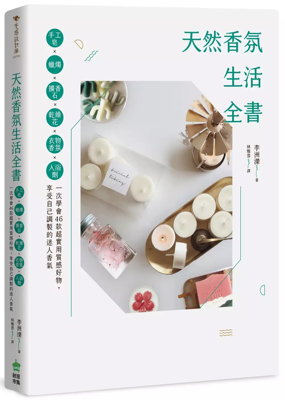
Ig pet的問題,我們搜遍了碩博士論文和台灣出版的書籍,推薦李洲濚寫的 天然香氛生活全書:手工皂x蠟燭x擴香石x乾燥花x衣物香氛x入浴劑,一次學會46款超實用質感好物,享受自己調製的迷人香氣 和Rob Thompson的 材質活用聖經:工業設計師必備的材質運用事典都 可以從中找到所需的評價。
另外網站Hashtags for #pet to grow your Instagram, TikTok也說明:Best hashtags for use with #pet are #pet #dog #pets #dogs ... Use one of these sets of hashtags in your next instagram post and you'll see a big boost.
這兩本書分別來自PCuSER電腦人文化 和旗標所出版 。
長庚大學 電子工程學系 賴朝松所指導 Mamina Sahoo的 基於石墨烯及生物碳基材料的可撓式電晶體應用與能量攫取 (2021),提出Ig pet關鍵因素是什麼,來自於石墨烯、氟化石墨烯、太阳能电池、摩擦纳米发电机、生物碳、能量收集器。
而第二篇論文高雄醫學大學 熱帶醫學碩士學位學程 師健民所指導 丹尼爾的 俄羅斯遠東地區城市家飼犬外寄生硬蜱之蜱滋生病原體的分子檢測 (2021),提出因為有 俄羅斯的重點而找出了 Ig pet的解答。
最後網站達人秀寵物(@pet.ttshow.tw) • Instagram photos and videos則補充:70.2k Followers, 111 Following, 4744 Posts - See Instagram photos and videos from 達人秀寵物(@pet.ttshow.tw) ... 7款必收藏「IG 動物GIF」 【讓你ㄉ限時一.
天然香氛生活全書:手工皂x蠟燭x擴香石x乾燥花x衣物香氛x入浴劑,一次學會46款超實用質感好物,享受自己調製的迷人香氣
為了解決Ig pet 的問題,作者李洲濚 這樣論述:
打造質感生活,用自己喜歡的顏色與香氛,做成分天然的香氛好物 一本入門新手也能輕鬆學會的手作學習書 【本書特色】 ◆零基礎也能學會的香氛手作 從製作工具、步驟作法、油品&蠟的種類、精油、用量、溫度皆有圖解詳細說明,跟著書中技巧學習,初學者也能輕鬆學會 ◆46款超實用居家、旅行攜帶生活好物 從手工皂的肌膚呵護,到蠟燭空間薰香、衣物香氛、個性香水、防蚊噴霧、去角質磨砂膏、車用芳香劑等,一次學會46款超實用生活香氛好物 本書帶你從香氛的基礎與應用、天然油品與蠟材挑選製作、色粉選擇添加, step by step圖解學會手工皂、香氛蠟燭、擴香石、乾燥花、空氣清新噴霧、泡澡入浴劑、寵物除臭、車
用芳香等多款香氛物品, 不論是春夏控油、秋冬保濕,給肌膚最佳滋潤與呵護的手工皂, 還是帶著淡淡春櫻花香的小茶燭,適合在秋天點燃的蜂蜜與肉桂柱狀蠟燭, 都可以隨心所欲打造出適合肌膚或自己喜歡的香氛物品,帶來好心情之餘也為家人健康把關。
Ig pet進入發燒排行的影片
期待的聲音 我聽見了 其實我早就錄製好了
使用各種不同剪刀的一集啦 哈哈
我相信多半新手 第一個遇到的挫折
就是直剪容易剪不好 開型開半天不敢下刀
直剪的容錯率是最低的 所以如果有容錯率高一點的剪刀
是不是在剪毛上的成功率會大大提升
阿貓跟你說答案是對的 不只成功率會提升 連速度都跟著會一起上漲
魚骨剪 魔術剪 等等等 很多啦 但記得 一分錢一分貨 阿貓直接跟你們說
不要拿2-3千塊的魔術剪 或者澎澎剪 跟我說 不好用阿
不要拿你連甚麼材質都不清楚的魚骨剪來跟我說 剪不了阿
選剪刀 要了解 品牌價值 刀刃設計 使用材料 產地 都攸關整體使用的感受
那麼文字分享到這邊 我們看影片吧~!!
寵愛寶貝 夢想開始
影片中阿貓愛用的器具購買連結
超好用小電剪
蝦皮下單連結🔗 https://shopee.tw/product/9308186/645...
無線磨甲器
蝦皮連結🔗 https://shopee.tw/product/9308186/633...
金色小彎剪 Dream夢-職人刀具 蝦皮連結
https://shopee.tw/product/9308186/298...
-----------------------------------------------
活動邀約 合作洽談 可以到這裡訊息
https://www.facebook.com/cat.dream.tw...
-----------------------------------------------
嗨大家好"我是只想專心做好美容的阿貓
美容經歷10餘年
高專注的注意力 與創造力 是最完美的特色
我是屬於大家的寵物造型師 努力為寵物美容帶來更多的歡樂與專業
------------------------------------------------------------
如果喜歡 歡迎點擊訂閱
想追蹤更多的阿貓貓
以下可以收尋到 更多 夢想寵物美容的一切
---------------------------------------
秘密IG https://www.instagram.com/dreampet040...
wechat cat198845
FB 粉絲團 https://www.facebook.com/cat.dream.tw...
FB個人 : https://www.facebook.com/dreampetsalo...
夢想直播DreamLive : https://www.facebook.com/DREAM.CAT.LI...
阿貓的部落格 : https://mthedogm1.pixnet.net/blog
基於石墨烯及生物碳基材料的可撓式電晶體應用與能量攫取
為了解決Ig pet 的問題,作者Mamina Sahoo 這樣論述:
Table of ContentsAbstract.......................................................................................................iFigure Captions........................................................................................xiTable Captions...................................................
....................................xxiChapter 1: Introduction1.1 Flexible electronics................................................................................11.2 Graphene the magical material ………………………….……….......21.2.1 Synthesis of graphene…………………………….….…...21.2.1.1 Mechanical exfoliati
on of graphene………………...……21.2.1.2 Epitaxial growth on Sic substrate………………….…..31.2.1.3 Chemical vapor deposition (CVD) method………….…..41.2.2 Graphene transfer…………………………………………....41.3 Application of graphene based Electronics……………………….......51.3.1 Graphene based flexible transparent electrode
……………….61.3.2 Top gated Graphene field effect transistor…………………….71.4 Challenges of flexible graphene based field effect transistors.……….91.5 Energy harvesting devices for flexible electronics………….........….91.6 Solar cell…………………………………………………………...101.6.1 Device architecture…………………………………………101.
6.2 Issues and Challenges of Perovskite solar cells………...121.7 Triboelectric nanogenerator (TENG)………………………………121.7.1 Working mode of TENG………………………………….141.8 Applications of TENG………………………………………………151.8.1 Applications of graphene based TENG…………………....151.8.2 Applications of bio-waste material ba
sed TENG………….171.9 Key challenges of triboelectric nanogenerator…………………....…191.10 Objective and scope of this study………………………………....19Chapter 2: Flexible graphene field effect transistor with fluorinated graphene as gate dielectric2.1 Introduction………………………………………………………....212.2 Material preparation a
nd Device fabrication………………. 232.2.1CVD Growth of Graphene on Copper Foil………………….232.2.2 Transfer of graphene over PET substrate……………...........252.2.3 Fabrication of fluorinated graphene ……………...........252.2.4 F-GFETs with FG as gate dielectric device fabrication……262.2.5 Material and electrical C
haracterization …………………272.3 Results and discussion…………………………………………….282.3.1 Material characterization of PG and FG……………...…...….282.3.2 Electrical characterization of F-GFET with FG as dielectrics..332.3.3 Mechanical stability test of F-GFET with FG as dielectrics ….362.4 Summary…………………………………………………
………....40Chapter 3: Robust sandwiched fluorinated graphene for highly reliable flexible electronics3.1 Introduction………………………………………………………….423.2 Material preparation and Device fabrication ………………….........443.2.1 CVD Growth of Graphene on Copper Foil…………………...443.2.2 Graphene fluorination …...…….…………
…………..............443.2.3 F-GFETs with sandwiched FG device fabrication....................443.2.4 Material and electrical Characterization…..............................453.3 Results and discussion ……………………………………...............453.3.1 Material characterization of sandwiched…………………….453.3.2 Electric
al characterization of F-GFET with sandwiched FG....473.3.3 Mechanical stability test of F-GFET with sandwiched FG…503.3.4 Strain transfer mechanism of sandwiched FG………………513.4 Summary…………………………………………………………....53Chapter 4: Functionalized fluorinated graphene as a novel hole transporting layer for ef
ficient inverted perovskite solar cells4.1 Introduction………………………………………………………….544.2 Material preparation and Device fabrication......................................564.2.1 Materials ………………………...…………………………564.2.2 CVD-Graphene growth ……………………………...…...564.2.3 Graphene fluorination …………………………………….564.
2.4 Transfer of fluorinated graphene…………………………...574.2.5 Device fabrication …………………………………….….574.2.6 Material and electrical Characterization …….....................584.3 Results and discussion …………………………………………….594.3.1 Surface electronic and optical properties of FGr……….….594.3.2 Characterization o
f FGr and perovskite surface ……….…644.3.3 Electrical performance of PSC………………….…….…...694.3.4 Electrical performance of Flexible PSC……………………724.4 Summary…………………………………………………………...78Chapter 5: Flexible layered-graphene charge modulation for highly stable triboelectric nanogenerator5.1 Introduction…………
…………………………………………....795.2 Experimental Section……………………………………………….825.2.1 Large-area graphene growth ……………………………….825.2.2 Fabrication of Al2O3 as the CTL …………………………...825.2.3 Fabrication of a Gr-TENG with Al2O3 as the CTL………825.2.4 Material characterization and electrical measurements…….835.3 Results
and discussion.…………………………………...…………845.3.1 Material Characterization of Graphene Layers/Al2O3……845.3.2 Working Mechanism of Gr-TENG with Al2O3 as CTL…915.3.3 Electrical Characterization of Gr-TENG with Al2O3 CTL…945.3.4 Applications of the Gr-TENG with Al2O3 as CTL……….1015.4 Summary…………………………………………
……………….103Chapter 6: Eco-friendly Spent coffee ground bio-TENG for high performance flexible energy harvester6.1 Introduction…………………………………………………….......1046.2 Experimental Section…………………………………………….1086.2.1 Material Preparation …………………………………….1086.2.2 Fabrication of SCG powder based TENG………………...1086
.2.3 Fabrication of SCG thin-film based TENG ………………1096.2.4 Material characterization and electrical measurements….1106.3 Results and discussion.…………………………………...………1116.3.1 Material Characterization of SCG powder and thin film….1116.3.2 Working Mechanism of SCG-TENG……………………...1186.3.3 Electrical Cha
racterization of SCG-TENG……………….1226.3.4 Applications of the SCG thin-film based TENG………….1326.4 Summary………………………………………………………….134Chapter 7: Conclusions and future perspectives7.1 Conclusion………………………………………………………....1357.2 Future work …………………………….………………………….1377.2.1 Overview of flexible fluorinated g
raphene TENG..............1377.2.1.1 Initial results………………………………….…1387.2.2.1.1 Fabrication of FG-TENG………………1387.2.2.1.2 Working principle of FG-TENG……….1397.2.2.1.3 Electrical output of FG-TENG.………...140References…………………………………………………………….142Appendix A: List of publications………………….……………..........177A
ppendix B: Fabrication process of GFETs with fluorinated graphene (FG) as gate dielectric……........……………………………………….179Appendix C: Fabrication process of GFETs with sandwiched FG…....180Appendix D: Fabrication process of inverted perovskite solar cell with FGr as HTL…………………………………………………………….181Appendi
x E: Fabrication of a Gr-TENG with Al2O3 as the CTL…….182Appendix F: Fabrication of SCG based triboelectric nanogenerator….183Figure captionsFigure 1-1 Exfoliated graphene on SiO2/Si wafer……………………….3Figure 1-2 Epitaxial graphene growth on SiC substrate………………....3Figure 1-3 Growth mechanism of graphe
ne on Cu foil by CVD ……......4Figure 1-4 Wet transfer process of CVD grown graphene…………...….5Figure 1-5 RGO/PET based electrodes as a flexible touch screen.……....6Figure 1-6 Graphene based (a) touch panel (b) touch-screen phone…….7Figure 1-7 Flexible graphene transistors (a) (Top) Optical photograph
of an array of flexible, self-aligned GFETs on PET. (Bottom) The corresponding schematic shows a device layout. (b) Schematic cross-sectional and top views of top-gated graphene flake–based gigahertz transistors. (Left) AFM image of a graphene flake. (Right) Photograph of flexible graphene devices
fabricated on a PI substrate. (c) Cross-sectional schematic of flexible GFETs fabricated using a self-aligned process……8Figure 1-8 The magnitude of power needed for meet certain operation depending critically on the scale and applications………………………10Figure 1-9 Schematic diagrams of PSC in the (a) n-i
-p mesoscopic, (b) n-i-p planar, (c) p-i-n planar, and (d) p-i-n mesoscopic structures………...12Figure 1-10 Schematic illustration of the first TENG...………………...13Figure 1-11 Working modes of the TENG. (a) The vertical contact-separation mode. (b) The lateral sliding mode. (c) The single-electrode mode
. (d) The free-standing mode ………………………………...……14Figure 1-12 Schematic illustration of (a) device fabrication of graphene-based TENGs (b) graphene/EVA/PET-based triboelectric nanogenerators (c) device fabrication of stretchable CG based TENG with electrical output performance……………………………………………………...17
Figure 1-13 Schematic illustration and output performance of bio-waste material based TENG (a) Rice-husk (b) Tea leaves (c) Sun flower powder (SFP) (d) Wheat stalk based TENG………….…………………………18Figure 2-1 Graphene synthesis by LPCVD method……….…………...24Figure 2-2 Schematic diagram of (a) preparation pro
cess of 1L-FG/copper foil (b) Layer by layer assembly method was used for fabricating three-layer graphene over copper foil and then CF4 plasma treatment from top side to form 3L-FG/copper foil…………………….26Figure 2-3 Schematic illustration of fabrication process of F-GFET with FG as gate dielectric ……
……………………………………………….27Figure 2-4 (a) Raman spectra of PG, 1L-FG and 3L-FG after 30 min of CF4 plasma treatment over copper foil. (b) Peak intensities ratio ID/IG and optical transmittance of PG, 1L-FG and 3L-FG. Inset: image of PG and 1L-FG film over PET substrate. (c) Typical Raman spectra of PG, 1L
-FG and 3L-FG on PET substrate. (d) Optical transmittance of PG, 1L-FG and 3L-FG film over PET substrate. The inset shows the optical image of GFETs with FG as gate dielectrics on PET ……….…………30Figure 2-5 XPS analysis result of (a) PG (b) 1L-FG (c) 3L-FG where the C1s core level and several carbon f
luorine components are labeled. The inset shows the fluorine peak (F 1s) at 688.5 eV……………………….32Figure 2-6 (a) Water contact angle of PG, 1L-FG and 3L-FG over PET substrate. (b) The relationship between water contact angle of PG, 1L-FG and 3L-FG and surface-roughness………………………………………33Figure 2-7 (a) I
d vs. Vd of w/o-FG, w/1L-FG and w/3L-FG samples after 30 min of CF4 plasma (b) Id vs. Vg of w/o-FG, w/1L-FG and w/3L-FG samples at a fixed value of drain to source voltage, Vds of 0.5 V (c) Gate capacitance of w/o-FG, w/1L-FG and w/3L-FG samples (d) Gate leakage current of w/o-FG (naturally formed A
l2OX as gate dielectric), w/1L-FG and w/3L-FG samples ……………………………...…………...……...34Figure 2-8 (a) Schematic illustration of bending measurement setup at different bending radius. (i) Device measurement at (i) flat condition (ii) bending radius of 10 mm (iii) 8 mm (iv) 6 mm. Inset shows the photograph
of measurement setup. Change in (b) carrier mobility (c) ION of w/o-FG, w/1L-FG and w/3L-FG samples as a function of bending radius. The symbol ∞ represents the flat condition. Change in (d) carrier mobility (e) ION of w/o-FG, w/1L-FG and w/3L-FG samples as a function of bending cycles (Strain = 1.
56%)…………………………………….38Figure 3-1 Schematic illustration of the flexible top gate graphene field effect transistor with sandwich fluorinated graphene (FG as gate dielectric and substrate passivation layer) ……………………………...…………44Figure 3-2 Raman spectra of (a) PG/PET and PG/FG/PET substrate (b) sandwiche
d FG (FG/PG/FG/PET). Inset showing the optical transmittance of sandwiched FG. (c) HRTEM image for 1L-FG.……………….….…46Figure 3-3 (a) Id vs. Vd of FG/PG/FG device at variable vg (−2 to 2 V). (b) Id vs. Vg of FG/PG/FG. (c) Gate capacitance of FG/PG/FG ….…….48Figure 3-4 Raman spectra of devices under be
nding (a) PG/PET (Inset shows the 2D peak) (b) PG/FG/PET (inset shows the 2D peak) …….…49Figure 3-5 (a) Change in Mobility (b) change in ION of PG/PET and PG/FG/PET as a function of bending radius between bending radii of ∞ to 1.6 mm in tensile mode (c) Change in Mobility (d) Change in ION of PG/PET
and PG/FG/PET as a function of bending cycles. Inset of (c) shows the photograph of F-GFETs with sandwich FG on the PET substrate (e) change in resistance of w/1L-FG, 1L-FG/PG/1L-FG samples as a function of bending radius ………………………...……………….50Figure 3-6 Schematic evolution of proposed strain transf
er mechanism through PG/PET and PG/FG/PET. The inset of PG/PET sample shows the generation of sliding charge due to interfacial sliding between PG and PET ………………………………………………………………….….52Figure 4-1 FGr fabrication and transfer process …………….………....57Figure 4-2 (a) Raman analysis of pristine graphene a
nd the FGr samples after 5, 10, 20, and 30 min of CF4 plasma treatment over Cu foil (b) Raman intensity ratios (I2D/IG and ID/IG) of fluorinated graphene, with respect to the exposure time ……………………………………………60Figure 4-3 SEM images of (a) ITO, (b) ITO/1L-FGr, (c) ITO/2L-FGr, and (d) ITO/3L-FGr …………………
………………………………….61Figure 4-4 XPS analysis of FGr with (a) 5 min (b) 10 min and (c) 20 min of CF4 plasma treatment on the Cu foil (d) The fluorine peak (F1s) of FGr (f) The correlation of the carbon-to-fluorine fraction (C/F) with exposure time and the corresponding carrier concentrations …………….………62Fi
gure 4-5 Tauc plots and UV–Vis absorption spectra of FGr films with CF4 plasma treatment for (a) 5, (b) 10, and (c) 20 min ….………......….63Figure 4-6 WCAs on PEDOT: PSS and 1L, 2L, and 3L FGr samples ...64Figure 4-7 (a) Mechanism of large grain growth of perovskite on a non-wetting surface (b) Top-vi
ew and cross-sectional surface morphologies of perovskites on various HTLs ………………………………...…………65Figure 4-8 XRD of perovskite films on various HTL substrates ….…...66Figure 4-9 UPS spectra of various numbers of FGr layers on ITO: (a) cut-off and (b) valance band spectra …………………………………….….67Figure 4-10
Energy band diagrams of PSCs with (a) PEDOT: PSS, (b) 1L-FGr, (c) 2L-FGr, and (d) 3L-FGr as HTL …………………….…….68Figure 4-11 (a) Steady state PL spectra of PEDOT: PSS/perovskite and FGr/perovskite films. (b) TRPL spectral decay of PEDOT: PSS/perovskite and FGr/perovskite films………………………….……69Figure 4-1
2 (a) Schematic representation of a PSC having an inverted device configuration. (b) Cross-sectional HRTEM image of the ITO/ FGr–perovskite interface………………………………………...………70Figure 4-13 Photovoltaic parameters of PSCs incorporating various HTL substrates: (a) PCE (%), (b) Voc (V), (c) Jsc (mA/cm2), an
d (d) FF (%)....71Figure 4-14 Normalized PCEs of target and control PSCs incorporating various HTL substrates, measured in a N2-filled glove box. (a) Thermal stability at 60 °C (b) Light soaking effect under 1 Sun (c) Stability after several days …………………………………………………………….72Figure 4-15 (a) Schematic r
epresentation of the structure of a flexible PSC on a PET substrate (b) J–V curves of control and target flexible PSCs, measured under both forward and reverse biases. (c) Average PCE of flexible PSCs incorporating PEDOT: PSS and FGr HTLs……….…73Figure 4-16 (a) Normalized averaged PCEs of the flexibl
e PSCs after bending for 10 cycles at various bending radii. (b) Normalized averaged PCEs of the flexible PSCs plotted with respect to the number of bending cycles at a radius of 6 mm ………………………………………………75Figure 4-17 Photovoltaics parameters of flexible PSCs with various HTL substrates: (a) JSC (mA/c
m2), (b) Voc (V), and (c) FF (%) ……………....75Figure 4-18 XRD patterns of perovskite films on PET/ITO/FGr, recorded before and after bending 500 times …………………………………….76Figure 4-19 SEM images of (a) perovskite films/FGr/ITO/PET before bending (b) after bending 500 times (c) perovskite films/PEDOT: PSS/
ITO/PET before bending (d) after bending 500 times ……………….…77Figure 4-20 PL spectra of perovskite films on PET/ITO/FGr, recorded before and after various bending cycles …………………………….…78Figure 5-1 Schematic illustration showing the fabrication process of a flexible Gr-TENG with Al2O3 as the CTL ……………
………………...83Figure 5-2 The Raman spectra of (a) graphene/Al-foil/PET and (b) graphene/Al2O3/Al-foil/PET. The I2D/IG of graphene layers (1L, 3L and 5L) over (c) Al-foil/PET substrate (d) Al2O3/Al-foil/PET substrate …...85Figure 5-3 XRD patterns of (a) graphene/Al-foil/PET and (b) graphene/Al2O3/Al-foi
l/PET ……………………………………………86Figure 5-4 FESEM image of the graphene surface on (a) Al-foil/PET and (b) Al2O3/Al-foil/PET. EDS analysis of (c) graphene/Al-foil/PET and (d) graphene/Al2O3/Al-foil/PET (e) EDS elemental mapping of the graphene/Al2O3/Al-foil/PET presenting C K series, O K series and Al K ser
ies …………………………………………………………….………87Figure 5-5 3D AFM images of (a) 1L-Gr (b) 3L-Gr (c) 5L-Gr on Al foil (d) 1L-Gr (e) 3L-Gr (f) 5L-Gr on Al2O3/Al foil………………….….….89Figure 5-6 Work function of graphene layers on the (a) Al-foil (b) Al2O3/Al-foil substrate by KPFM. Inset showing the surface potential of
graphene layers (1L, 3L and 5L) over Al-foil and Al2O3 substrate (c) energy band diagrams for 1L-Gr, 3L-Gr and 5L-Gr over Al2O3 ……....90Figure 5-7 Schematic illustration of Electronic energy levels of graphene samples and AFM tip without and with electrical contact for three cases: (i) tip and the
1L-Gr (ii) tip and the 3L-Gr and (iii) tip and the 5L-Gr over Al2O3/Al foil/PET……………………………………….…...…………91Figure 5-8 Working mechanism of Gr-TENG with Al2O3 ….….…...…93Figure 5-9 a) ISC and (b) VOC of 1L-, 3L- and 5L-Gr-TENGs without Al2O3 CTL (c) Sheet resistance of graphene as a function of number
of layers ………………………………...…...…………………………….95Figure 5-10 Electrical output of the Gr-TENG with Al2O3 CTL: (a) ISC and (b) VOC of 1L-, 3L- and 5L-Gr. Magnification of the (c) ISC and (d) VOC of the 3L-Gr-TENG with Al2O3 as the CTL. Average mean (e) ISC and (f) VOC generated by pristine Gr-TENGs (1L, 3L
and 5L) and Gr-TENGs (1L, 3L and 5L) with Al2O3 CTL. Error bars indicate standard deviations for 4 sets of data points ……………...…………….….…......96Figure 5-11 (a) CV of Al/Al2O3/3L-Gr/Al at 100 kHz and 1 MHz (b) CV hysteresis of 3L-Gr-TENG with Al2O3 as CTL with different sweeping voltages (c) Surface
charge density of graphene (1L, 3L and 5L)-based TENG with and without Al2O3 as CTL ………………………………...98Figure 5-12 Circuit diagram of output (a) VOC and (b) ISC measurement of 3L-Gr TENG with Al2O3 CTL as a function of different resistors as external loads. Variation in VOC and ISC w.r.t different re
sistors as external loads of (c) 3L-Gr TENG with Al2O3 CTL (d) 3L-Gr TENG without Al2O3 CTL. Relationship between electrical output power and external loading resistance (e) 3L-Gr TENG with Al2O3 CTL (f) 3L-Gr TENG without Al2O3 CTL…………………………………….………………...99Figure 5-13 (a)Electrical stability and du
rability of the 3L-Gr TENG with Al2O3 (b) Schematic illustrations showing the charge-trapping mechanism of 3L-Gr-TENG without and with Al2O3 charge trapping layer ………101Figure 5-14 (a) Photograph showing 20 LEDs being powered (b) Circuit diagram of bridge rectifier (c) Charging curves of capacitors
with various capacitances (d) Photograph of powering a timer …….………………102Figure 6-1 The schematic diagram of the fabrication process for SCG powder based TENG ……………………………………………….….108Figure 6-2 The schematic diagram of the fabrication process for SCG thin-film based TENG via thermal evaporation meth
od ………………109Figure 6-3 FESEM image of (a) SCG powder (inset image illustrates the high magnification of SCG powder) (b) SCG thin-film/Al foil/PET (inset image illustrates the high magnification of SCG thin-film). EDS of the (c) SCG powder (d) SCG thin-film/Al foil/PET…………………………. 112Figure 6-4 Raman
spectra analysis (a) pristine SCG powder (b) SCG thin-film/Al foil/PET. XRD patterns of (c) SCG powder (d) SCG thin film with different thickness ……………………………………… ……….115Figure 6-5 FTIR analysis of the (a) pristine SCG powder sample (b) SCG thin film………………………………………………………………...116Figure 6-6 3D AFM ima
ge of SCG thin-film with various thickness (a) 50 nm (b)100 nm and (c) 200 nm……………………………………...117Figure 6-7 Schematic illustration of working principle of SCG thin-film based TENG …………………………………………………………...119Figure 6-8 Finite element simulation of the generated voltage difference for SCG thin-film b
ased TENG based on the contact and separation between SCG thin film and PTFE …………….……………………….120Figure 6-9 (a) The setup for electrical property testing, which including a Keithley 6514 system electrometer and linear motor. Electrical output (b) ISC (c) VOC of TENGs based on different friction pairs
for checking the triboelectric polarity of SCG…………………………………………...123Figure 6-10 Electrical measurement of (a) ISC and (b) VOC of the SCG thin-film based TENG. Mean value of (d) ISC (e) VOC and (f) Output power density of the pristine SCG powder and thermal deposited SCG thin-film based TENG. ...………
………………………………………125Figure 6-11 (a) Schematic illustration of KPFM for measuring the work function. (b) Surface potential images of SCG thin film with various thickness (50 nm, 100 nm and 200 nm). (c) Surface potential and (d) Work function vs SCG thin film with various thickness (50 nm, 100 nm and 20
0 nm).………….……………………………………………….128Figure 6-12 (a) Isc and (b) Voc of SCG thin film based TENG under different contact frequencies (c) Isc and (d) Voc of SCG thin film based TENG under different separation distance…………………………….129Figure 6-13 Electrical response (a) ISC (b) VOC of pristine SCG powder an
d (c) ISC (d) VOC of SCG thin-film based TENG with respect to different relative humidity (35-85% RH) …………………………….131Figure 6-14 Electrical stability and durability test of the output performance of (a) pristine SCG powder based TENG (b) SCG thin-film based TENG……………………………………………………………132Figure 6-15
Applications of the SCG thin film based TENG as a power supply: (a) Circuit diagram of the bridge-rectifier for charging a capacitor (b) Charging curves of capacitors with various capacitances (0.1, 2.2 and 3.3 µF) (c) Photograph of powering a timer…………………...………133Figure 7-1 Schematic illustration o
f FG based TENG…….….……….139Figure 7-2 Working mechanism of FG based TENG…………………140Figure 7-3 Electrical output of FG-TENG: (a) Isc and (b) Voc …….….141Table captionsTable 2-1 Comparison of flexible G-FETs on/off ratio of our work with other’s work…………………………………………………...………...40Table 3-1 Summary of th
e electrical and mechanical performance of flexible w/o-FG, w/ 1L-FG, w/3L-FG and sandwich FG (FG/PG/FG) samples......................................................................................................52Table 3.2: Comparison of the electrical and mechanical performance of sandwich FG ba
sed F-GFET with previous F-GFET with different gate dielectrics……………………………………………………….………53Table 4-1 Best photovoltaic performance from control and target devices prepared on rigid and flexible substrates……………………………......74Table 5-1 EDS elemental analysis of graphene over Al-foil/PET and Al2O3/Al-foi
l/PET ………………………………………………………88Table 5-2 Comparison of electrical output performance of Gr-TENGs with and without Al2O3 CTL samples used in this study………………103Table 6-1 EDS elemental analysis of SCG-Powder and SCG thin film /Al foil/PET………………………………………………………………...113Table 6-2 Comparison of electrical o
utput performance of SCG-TENGs samples used in this study……………………………………………...126
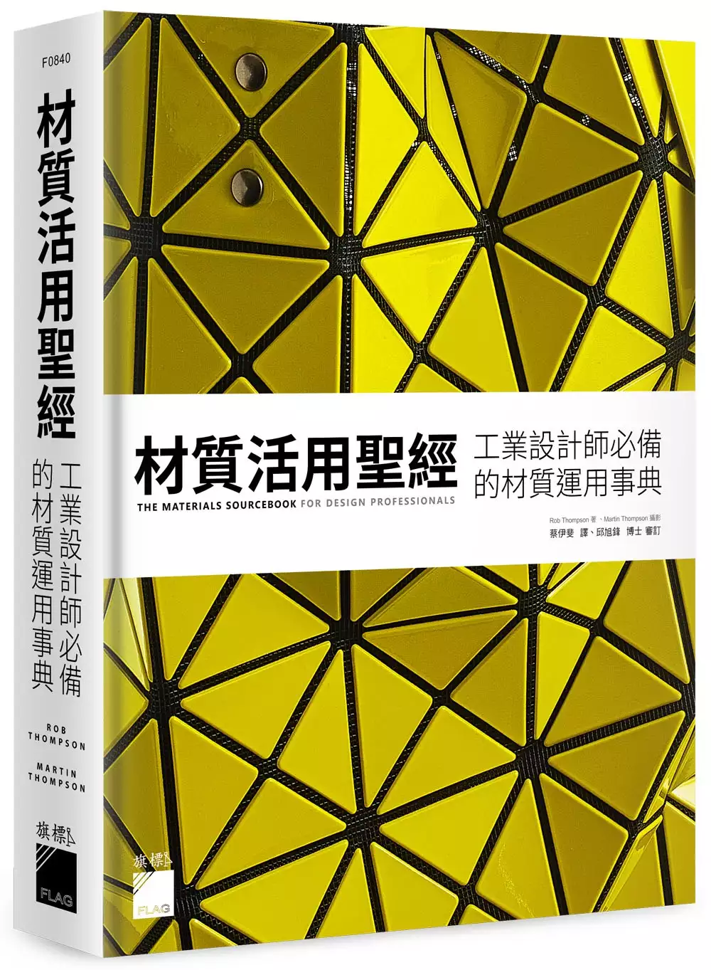
材質活用聖經:工業設計師必備的材質運用事典
為了解決Ig pet 的問題,作者Rob Thompson 這樣論述:
本書提供各類常見材質的應用方法等知識,能幫助設計師們為作品選擇最適合的材質。找到對的材質不只能導引出更好的設計成果,同時也能將製造過程中耗損的能源與產生的廢料降至最低。隨著各種材質的應用範圍不同,本書中豐富多樣的資訊可讓設計師擁有無限的可能。 本書分為六章,每章代表一種常見材質:第一部份為金屬、第二部份為塑膠、第三部份為木材、第四部份為植物、第五部份為動物、第六部份為礦物。每一章中提到材質時,都會以最常應用該材質的產業為例去分類探究。除此之外,書中亦穿插了 98 個補充說明區塊,談及上百種材質,並加上精彩且美觀的的應用實例,示範每種材質的屬性與設計上的可能性。
為了幫助讀者選擇,本書在介紹每種材質時,第一步都是介紹該材質在相容性上的注意事項,包括製作過程中以及與其他材質搭配時的相容性。書中選出的範例會展示該材質最獨特的屬性與特徵,但這只是設計案的起點,最後要如何應用在專案上,仍由設計者依幾何形狀、數量、成本、可用性和其他各種因素來評估。 舉例來說,某些材質原本就具有能與設計搭配的光滑表面,但其他材質則需要另作表面處理來保護媒材;設計者若能了解各材質本身的表面狀況、觸感與物理特性,可提升設計專案的廣度。書中將提供各種材質需要考慮的面向與示範案例,包括該材質使用後回收的可能性。 目前設計方法與技術不斷進步,許多材質在使
用壽命終止後,仍然有可能是珍貴的商品。由於立法、行政命令、巧妙的設計施工.......等原因,不難見到材料不斷重複使用的案例,我們若能將資源集中起來避免製造污染,可讓這個循環更有效率,也更符合永續發展。本書中也會提供建議的處理方法,協助你在製造產品和環保之間取得平衡。 本書特色 ★找到對的材質,產品才會更完美! 產品設計、工業設計人隨時都需要的材質活用聖經,一書在手,即可掌握世間所有材質的活用方法,讓你創作時更加得心應手,甚至從材料中找到創作的靈感! ★不怕看不懂!中文版使用台灣業界用語 本書中文版特別聘請材料科學專家審校,補充台灣業
界常用的材質種類、用語、應用方式等,期許更符合台灣的使用情境。 ★只有想不到,沒有找不到的材質! 本書分為金屬、塑膠、木材、植物、動物、礦物等六大章節,幾乎涵蓋了所有的常見材質。每一種材質的說明頁皆提供仔細的成分表、強度表、與競爭材質的比較表、實際使用案例等,便於查詢與參考。 ★使用大家熟悉的知名產品作為範例,就算你不懂材質,也能從翻閱中獲得許多產品知識 ◆主婦們爭相採購的琺瑯鑄鐵鍋,探究好用的原理 (金屬篇) ◆日本傳統刀具「三德刀」的妙用 (金屬篇) ◆iPhone 4 為什麼採用不鏽鋼手機底座 (金屬篇) ◆PUMA
「RS100 INJEX」運動鞋用 EVA 泡棉製成鞋底,加強彈性和耐衝擊強度 (塑膠篇) ◆三宅一生最有名的「Bao Bao」購物袋,使用三角型 PVC 板包覆 PET 底材 (塑膠篇) ◆Uniqlo 連帽羽絨外套採用精紡聚醯胺長絲,讓表面具防潑水功能,且有卓越的彈性與耐磨性,使超輕表布能折疊收入極小的收納袋 (塑 膠篇) ◆白楊木薄板沒有特殊氣味,適合製成起士用木盒 (木材篇) ◆竹蒸籠這種炊具已在中國流行數千年,即使後來出現各種現代炊具,仍流傳到世界各地(植物篇) ◆羊毛氈目前可製成各種生活用品,好處是不用紡織,而且製品堅固密實 (動物篇)
◆滑石具有裝飾功能,常用於建築和雕塑,最有名的例子是俯瞰里約熱內盧的基督救世主雕像 (礦物篇) 讀者書評 ◆ Amazon.com 5 星推薦!產品設計師 / 工業設計師必備的材質工具書! 「每位設計師都應該擁有這本書。翻閱它就像環遊世界,能接觸到全世界數百名設計師的集體創意,他們已經達到設計藝術的頂峰:能讓材質轉化為高水準的產品。我們非常喜歡並強烈推薦本書。每間設計圖書館都應該要擁有這本書。」---美國工業設計雜誌《Innovation Magazine》 ★知名設計師、設計科系教授一致推薦 「設計師應該都要準備一本這樣的參
考書。」---吳俊延 Ocean MAX 設計總監 (曾任崇右影藝科技大學 專任副教授兼設計學院院長) 「當你越貼近這份材質,越深入理解這項工藝,設計上將沒有任何限制。」---林靖格 gridesign studio 格子設計創辦人/設計總監 「選擇對的、好的、新的材質,絕對會讓設計創意加分的;本書提供了便捷的創意參考,且有助於開啟創意想像,值得您珍藏、活用!」---官政能 實踐大學工業產品設計系 榮譽講座教授 (曽任 副校長、設計學院 創院院長) 「創新的產品需要搭配合適的材質應用,工業設計師可隨時參考這本『聖經級』的材質寶典,內容包含各類材質
特性的說明與案例應用經驗,對於所設計的產品將更有提昇品質的功用。」---陳建雄 國立臺灣科技大學設計系 教授/系主任 「關於材質我花了三十年還學不透, 這本書一一系統化完整解析。」---謝榮雅 奇想創造董事長 (生涯累計獲得超過百座國際大獎,被譽為「台灣工業設計教父」) 作者簡介 羅伯.湯普森 羅伯.湯普森(Rob Thompson)是材料與製程領域的專家。 在過去20年中,羅伯以設計師的角色活躍於材料與製程的相關領域,包括學術研究以及如何創造新產品與新材料等。他從英國中央聖馬汀藝術學院畢業後,曾先後任職於多家國際知名大廠,包括:L
G 電器、P&G、Panasonic、Nokia 等。他在擔任Nokia首席設計師的四年時間裡,率先採用了以材料主導設計的方法,並且憑藉其「色彩與材料設計策略研究 (Colour and Material Design Strategy)」在 2013 年榮獲國際傑出工業設計金獎(IDEA)和美國工業設計師協會金獎 (IDSA)。 羅伯目前已推出多本產品設計相關著作,皆是產品設計相關人士必讀的重要經典,例如《Product and Furniture Design (The Manufacturing Guides)》 (中文版書名為《產品製造工法入門: 產品+家具設計篇》(龍溪
圖書),本書就是他的最新力作,將他對產品材質的知識完全傳授給讀者。 審訂者簡介 邱旭鋒 國立清華大學材料科學工程學系博士 Dr. Chiu 於電子陶瓷材料研究超過十年經驗,多篇研究成果發表於國際知名期刊,專長為半導體元件製程、材料物性與電性分析。在業界多年專案(新事業)開發管理經驗,跨足材料、光電、通訊、生醫。致力於結合新技術為商業帶來更多想像。 IG: jimmy.chiu_official 譯者簡介 蔡伊斐 文藻外語學院畢業,旅居海外多年,專職攝影,熱愛翻譯與文字創作,譯有《設計政治學》、《符號的故事
》、《脫穎而出的品牌致勝秘密 2》、《Flying Colors國旗的故事》、《設計準則:Massimo Vignelli》等書。 第一章 金屬 第二章 塑膠 第三章 木材 第四章 植物 第五章 動物 第六章 礦物
俄羅斯遠東地區城市家飼犬外寄生硬蜱之蜱滋生病原體的分子檢測
為了解決Ig pet 的問題,作者丹尼爾 這樣論述:
研究背景: 蜱滋生感染症在俄羅斯遠東地區成為主要公衛考量,其中有關蜱媒介立克次體菌、疏螺旋體、邊蟲及艾立克體等致病原皆常被臨床醫師所忽略。而立克次體菌及其他病原體皆已存在於各種病媒蜱及鄉村地區之野生哺乳類動物,然而卻無任何研究探討這些致病原於城市環境之家飼動物狀況。研究目的: 本研究於2021年6月至8月自俄羅斯遠東地區之哈巴羅夫斯克市(Khabarovsk)進行家飼犬外寄生蜱隻採集,並依其形態特徵進行蜱種確認,並進行立克次體菌、伯氏疏螺旋體、血小板邊蟲及犬艾立克體等病原體在蜱隻之感染篩檢。研究方法: 本研究之蜱隻乃採集自哈巴羅夫斯克市三個地區之獸醫院,採集得之蜱隻依其形態學主要特徵於立體解
剖顯微鏡下確認蜱種。而每一蜱隻則使用核酸萃取試劑組(DNeasy Blood & Tissue Kit)進行核酸(DNA)萃取,隨後運用巢式/半巢式聚合酶鏈反應技術(nested/seme-nested PCR)分別針對立克次體菌之gltA/ompB/ompA/17kd基因、血小板邊蟲及犬艾立克體之16SrRNA及伯氏疏螺旋體之OspA and 5S-23S intergenic spacer基因進行蜱隻之感染篩檢。而陽性樣本則進一步送定序。研究結果: 總計有140蜱隻採集自24隻家飼犬,並確認三屬四種株之硬蜱,包括11隻 (7.9%) 全溝硬蜱(Ixodes persulcatus)、62隻
(44.3%) 嗜群血蜱(Haemaphysalis concinna) 、10 隻(7.1%) 日本血蜱(Haemaphysalis japonica) 、55隻 (39.3%) 森林革蜱(Dermacentor silvarum)及2隻 (1.4%) 破損無法確認蜱種。其中包括66 隻(47.2%) 雄蜱、70 隻(50.0%) 雌蜱、3 隻(2.1%) 稚蜱及1隻 (0.7%)因蜱體破損而無法確認。經立克次體菌基因篩檢後發現共有32隻(22.8%)蜱感染立克次體菌,其中包括12隻(8.6%)嗜群血蜱(H. concinna)、9 隻(6.4%) 全溝硬蜱(I. persulcatus)
、 8隻 (5.7%) 森林革蜱(D. silvarum)及 3隻 (2.1%) 日本血蜱(H. japonica)。而全部陽性感染樣本則包含10 隻(7.1%) 雄蜱及22隻 (15.7%)雌蜱,並沒有任何稚蜱檢測到Rickettsia感染。依據定序結果顯示陽性樣本分別與Rickettsia heilongjiangensis 或 Candidatus Rickettsia tarasevichiae兩基因種株具有100%基因相似度,無任何樣本檢測到疏螺旋體、邊蟲及艾立克體感染。討論: 本研究結果確認所有曾發現於俄羅斯遠東地區之蜱種,並以嗜群血蜱(H. concinna)為主要蜱種,而四種蜱
種皆可檢測到立克次體菌感染,整體陽性率與鄰近國家(例如:中國及南韓)相似,因此,本研究首次確認俄羅斯遠東地區城市犬類宿主之外寄生硬蜱存在感染R. heilongjiangensis 及 Candidatus Rickettsia tarasevichiae兩種立克次體菌之基因種株。